- 您现在的位置:买卖IC网 > Sheet目录369 > W971GG6JB25I (Winbond Electronics)IC DDR2 SDRAM 1GBIT 84WBGA
�� �
�
�W971GG6JB�
�8.6�
�Precharge� operation�
�The� Precharge� Command� is� used� to� precharge� or� close� a� bank� that� has� been� activated.� The�
�Precharge� Command� can� be� used� to� precharge� each� bank� independently� or� all� banks� simultaneously.�
�Three� address� bits� A10,� BA0� and� BA1� and� BA2� are� used� to� define� which� bank� to� precharge� when� the�
�command� is� issued.�
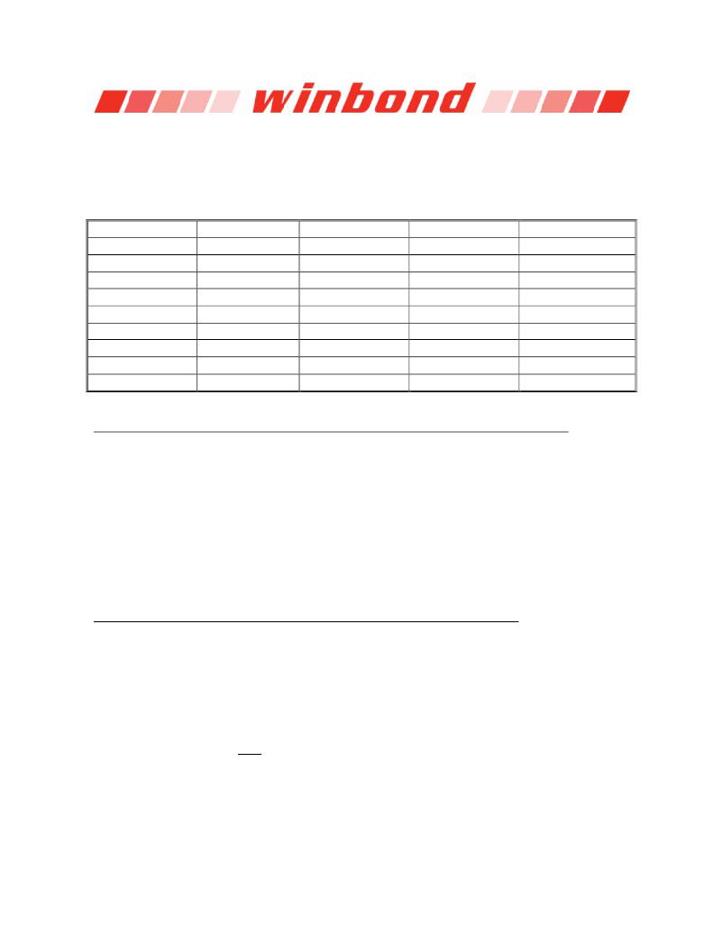
�Table� 4� –� Bank� selection� for� precharge� by� address� bits�
�A10�
�LOW�
�LOW�
�LOW�
�LOW�
�LOW�
�LOW�
�LOW�
�LOW�
�HIGH�
�BA2�
�LOW�
�LOW�
�LOW�
�LOW�
�HIGH�
�HIGH�
�HIGH�
�HIGH�
�Don� ?� t� Care�
�BA1�
�LOW�
�LOW�
�HIGH�
�HIGH�
�LOW�
�LOW�
�HIGH�
�HIGH�
�Don� ?� t� Care�
�BA0�
�LOW�
�HIGH�
�LOW�
�HIGH�
�LOW�
�HIGH�
�LOW�
�HIGH�
�Don� ?� t� Care�
�Precharge� Bank(s)�
�Bank� 0� only�
�Bank� 1� only�
�Bank� 2� only�
�Bank� 3� only�
�Bank� 4� only�
�Bank� 5� only�
�Bank� 6� only�
�Bank� 7� only�
�All� Banks�
�8.6.1�
�Burst� read� operation� followed� by� precharge�
�Minimum Read to Precharge command spacing to the same bank = AL + BL/2 + max(� RTP� , 2) - 2 clks�
�For� the� earliest� possible� precharge,� the� precharge� command� may� be� issued� on� the� rising� edge� which�
�is� “Additive� Latency� (AL)� +� BL/2� +� max(� RTP� ,� 2)� -� 2� clocks”� after� a� Read� command.� A� new� bank� active�
�(command)� may� be� issued� to� the� same� bank� after� the� RAS� precharge� time� (t� RP� ).� A� precharge�
�command� cannot� be� issued� until� t� RAS� is� satisfied.�
�The� minimum� Read� to� Precharge� spacing� has� also� to� satisfy� a� minimum� analog� time� from� the� rising�
�clock� edge� that� initiates� the� last� 4-bit� prefetch� of� a� Read� to� Precharge� command.� This� time� is� called�
�t� RTP� (Read� to� Precharge).� For� BL� =� 4� this� is� the� time� from� the� actual� read� (AL� after� the� Read�
�command)� to� Precharge� command.� For� BL� =� 8� this� is� the� time� from� AL� +� 2� clocks� after� the� Read� to� the�
�Precharge� command.� (Example� timing� waveforms� refer� to� 11.15� to� 11.19� Burst� read� operation�
�followed� by� precharge� diagram� in� Chapter� 11)�
�8.6.2�
�Burst� write� operation� followed� by� precharge�
�Minimum Write to Precharge Command spacing to the same bank = WL + BL/2 clks + t� WR�
�For� write� cycles,� a� delay� must� be� satisfied� from� the� completion� of� the� last� burst� write� cycle� until� the�
�Precharge� Command� can� be� issued.� This� delay� is� known� as� a� write� recovery� time� (t� WR� )� referenced�
�from� the� completion� of� the� burst� write� to� the� precharge� command.� No� Precharge� command� should� be�
�issued� prior� to� the� t� WR� delay.� (Example� timing� waveforms� refer� to� 11.20� to� 11.21� Burst� write� operation�
�followed� by� precharge� diagram� in� Chapter� 11)�
�8.7�
�Auto-precharge� operation�
�Before� a� new� row� in� an� active� bank� can� be� opened,� the� active� bank� must� be� precharged� using� either�
�the� Precharge� command� or� the� Auto-precharge� function.� When� a� Read� or� a� Write� command� is� given�
�to� the� DDR2� SDRAM,� the� CAS� timing� accepts� one� extra� address,� column� address� A10,� to� allow� the�
�active� bank� to� automatically� begin� precharge� at� the� earliest� possible� moment� during� the� burst� read� or�
�write� cycle.� If� A10� is� LOW� when� the� READ� or� WRITE� command� is� issued,� then� normal� Read� or� Write�
�burst� operation� is� executed� and� the� bank� remains� active� at� the� completion� of� the� burst� sequence.� If�
�A10� is� HIGH� when� the� Read� or� Write� command� is� issued,� then� the� Auto-precharge� function� is�
�engaged.� During� Auto-precharge,� a� Read� command� will� execute� as� normal� with� the� exception� that� the�
�Publication� Release� Date:� Sep.� 24,� 2013�
�-� 27� -�
�Revision� A09�
�发布紧急采购,3分钟左右您将得到回复。
相关PDF资料
W971GG8JB-25
IC DDR2 SDRAM 1GBIT 60WBGA
W9725G6IB-25
IC DDR2-800 SDRAM 256MB 84-WBGA
W9725G6JB25I
IC DDR2 SDRAM 256MBIT 84WBGA
W9725G6KB-25I
IC DDR2 SDRAM 256MBIT 84WBGA
W972GG6JB-3I
IC DDR2 SDRAM 2GBITS 84WBGA
W9751G6IB-25
IC DDR2-800 SDRAM 512MB 84-WBGA
W9751G6KB-25
IC DDR2 SDRAM 512MBIT 84WBGA
W9812G6JH-6I
IC SDRAM 128MBIT 54TSOPII
相关代理商/技术参数
W971GG6JB-25I
制造商:Winbond Electronics 功能描述:-40~85 1GB DDR2 FOR INDUSTRY
W971GG6JB25ITR
制造商:Winbond Electronics Corp 功能描述:1G, DDR2-800, X16, IND TEMP
W971GG6JB25TR
制造商:Winbond Electronics Corp 功能描述:NR, DDR2-800, X16
W971GG6JB-3
制造商:Winbond Electronics Corp 功能描述:1GBIT DDRII
W971GG6KB-18
制造商:Winbond Electronics Corp 功能描述:1G, DDR2-1066, X16 制造商:Winbond Electronics Corp 功能描述:IC MEMORY
W971GG8JB
制造商:WINBOND 制造商全称:Winbond 功能描述:16M × 8 BANKS × 8 BIT DDR2 SDRAM
W971GG8JB-25
功能描述:IC DDR2 SDRAM 1GBIT 60WBGA RoHS:是 类别:集成电路 (IC) >> 存储器 系列:- 标准包装:72 系列:- 格式 - 存储器:RAM 存储器类型:SRAM - 同步 存储容量:4.5M(256K x 18) 速度:133MHz 接口:并联 电源电压:3.135 V ~ 3.465 V 工作温度:0°C ~ 70°C 封装/外壳:100-LQFP 供应商设备封装:100-TQFP(14x20) 包装:托盘
W9725G6IB-25
功能描述:IC DDR2-800 SDRAM 256MB 84-WBGA RoHS:是 类别:集成电路 (IC) >> 存储器 系列:- 标准包装:1,000 系列:- 格式 - 存储器:EEPROMs - 串行 存储器类型:EEPROM 存储容量:4K (512 x 8) 速度:400kHz 接口:I²C,2 线串口 电源电压:2.7 V ~ 5.5 V 工作温度:-40°C ~ 85°C 封装/外壳:8-SOIC(0.173",4.40mm 宽) 供应商设备封装:8-MFP 包装:带卷 (TR)